Category Archives: Rbt Houdin’s house of magic

Make your own 3D HoloMonitor

A recent search on github for code relating to stereo 3D photogramertitry and synthetic computer generated holograms. lead me to the paper Holovideo on a stick, Integrated Optics for Holographic Video Displays by Daniel E. Smalley[1]

Most intriguing was the statement “If you want a Hologram video monitor, you have to make it yourself. Now I love do it your self projects. Ones that are most complicated. Not that I need another project, I have enough as is to keep me occupied for at least 500 years. In a way this is one of them. I always wanted to make my own hologram. My interests in Holography date back to the 1960s and the exhibits in the Exploratorium and the Laserium. In may ways such a device, would actually help in the other projects, giving a tool to use in visualizing how such things as the Antikeythera device, or Babbage’s computer are designed to work.

MIT has made much of their research available on github[3] with the admonition “We hope that hobbyists and researchers around the world can be inspired by and use this code to help achieve the goal of creating high-quality consumer holo video displays.”

Is this a practical statement? Can one make a Holographic Video monitor? After reading through the paper I would say a qualified ‘yes.’ There are a number of broken or incomplete links on the website. A note pointing out these broken links, to Dr Smalley public email address, was not quickly answered. It does not seem that there has been much publicly shared since 2014. There are some impressive You tube videos, which only seem to have 14 or so views. None of the links to the Mark-V version of the project work other than showing a plexiglass case.

The Mark-IV project is well documented. This seems to relate directly to Dr Smalley’s thesis[1]. I found this thesis to be lucid and well, written and thought out. It really does imply that one can make a Holographic video monitor. Much of this reminds me of computing in the early 1970s. And the 3D printer craze in the late 2000s.

Dr Smalley and his team have broken down the design into a series of sub modules. One of which is an Arduino. Of these modules the easiest item to source is the floating coin (or floating frog illusion.) This was a popular attraction at the Exploratorium. This curved reflector also gives the display it’s distinctive look.

The electronic modules also look fairly easy to replicate. I have done a lot of printed circuit boards. The first SMT PCB I did in the early 2000s was for a surplus LCD camcorder video display, which required obsolete parts distributed amongst the overstock dealers. These were from a 1990s era Cybermaxx Virtual reality headset. One of these headsets can be seen in the opening scenes of the movie _Titanic_. Where the sub operator is exploring the wreck.

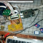
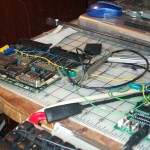
Andrew Henrie’s[2] documentation of the Mark-IV display refers to PCBs as CCAs, Which I take to mean Circuit Card Assembly. I will retain this terminology for the completed assembly. These CCAs are both well documented and obscurely sketchy. There are photographs of the PCBs as well as links to the data sheets of the chips involved. Nowhere is a schematic with Bill of materials, or any sort of layout pdf, or Gerber. One of the CCAs is an Arduino with shield. From the photographs the shield is simply a solder-less prototyping breadboard. The function is to support a DAC.

Not well documented is the post amp that the DAC uses to drive the Galvanometer. The closest thing to a schematic is an online simulation of the synchronization CCA with an absurdly long link. This Java applet surprisingly works well, and can be saved offline, incase the website goes down. This sim applet may be useful in the future should one want to simulate simple circuits, without a full blown spice model. It is not clear the photographs show hex switches which I actually have some of in my junk box. There is also a spectra stripe ribbon cable who’s function is not apparent, as well as a bank of electrolytic caps.

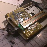
It is evident that much of this prototype is made from surplus parts. I love surplus stuff. Of the surplus items, used in the Mark-IV sub-assemblies, I am most familiar with the Polygon Mirror unit. I worked for most of the 1990s at Apple Imaging, where I wrote tests in postscript for the laserwriters. Some of us were also into robotics and we were given permission to go through the trash recycle for project parts. When the prototype printers were scrapped, a screwdriver was driven into this assembly to smash the laser optics. Still one had access to the sensors and servos to play with, as well as the data sheets giving the specifications. These were either made by Cannon or Fuji Xerox. From the marking in [2] it looks like a Fuji Xerox unit from a Sharp printer is used.

Laser-printers have a consumables lifespan of about 7 years. This means that the polygon units are somewhat available in the surplus markets. Pretty much for cheap if not free. There is also a tendency to put these into storage when their usefulness expires. These then get donated to co-ops and other shared resorce projects.

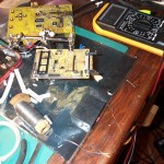
The local maker-space broke up a dozen or so printers for the gearing, stepper and servo motors. I have used the rollers in my crank organ and piano roll scanning projects. The screws and springs are also quite useful. I found one of these polygon units in a junk box at the local maker space. These were pulled from copy scanners (Probably HP) most of the polygons have 4 sides. I found one with 6 faces. An online search located the motor driver chip datasheet. There are a number of videos of polygon assemblies being run off arduino boards to create the PWM frequency needed. Also in the junk box were a number of planar mirrors.

Markings in the photographs[2] show the exact model of the Galvanometer used. A search of this part number currently shows this to still be a popular eBay item. Although a bit on the pricy side. These units seem to be used in point of sale grocery scanners. The tricky part would be to source the lightweight mirror, which is a section of aluminized silicon wafer. It may be possible to use one of the junk box mirrors ground down. The next group of assemblies to look at start with the Amplifier CCA. Again there is no schematic or board layout other than the photographs. The parts are given as data sheets. There is also a Carrier CCA, which it is indicated was not used in the documented project. The Amplifier board being directly driven by a fairly common NVIDIA GPU board. Such GPU boards also currently seem to be on eBay.

In reference [2] There is a whole appendix on debugging the amplifier board. Photographs show a hand soldered surface mount PCB. Having done home made SMT PCBs for over 20 years I can see the over abundance of excess solder on the component leads. A reflow oven and a proper solder paste mask would probably be on order here. Like the synchronization CCA the parts used on the amplifier CCA are easy to source through the main line distributers.

Now we come to the tricky part, which could be a real show stopper. This is the Acousto-Optic Modulator. Maddeningly the paper gives a specific part number. Which comes up ‘not found.’ or ‘Not available.’ A call to the manufacture asking for a data sheet an possible purchase was pleasantly responded to, however at the time of this review, a return call from an engineer has not happened.

Acousto-Optic Modulator’s are for sale on eBay ranging from 50USD, to over a thousand USD. There is not any documentation on these units. It looks like one would have to put a pin in it and order one blind to see what it does. It may be that quite a few channels are needed. There are references to 18 channels. The online search algorithms are not fine enough to separate out anything relating to channels. Searches for Acouso-optical modulator and Bragg cells return the same results.

It is evident that the Acousto-Optic Modulator is Dr Smalley’s first love. In his thesis he details the design and manufacture of such devices optimized for Holographic display use. It really does make one feel like one could follow the instructions. That it would be as easy to build as an adirondack lawn chair.

Now people like Jerri Elseworth and Sam Zeloof have built chips in their garage. I suspect there are others. Even I have acquired some surplus chip making equipment, which I used to make the Adelmous Fey mechanical doll[4]. As well as extending some of my watchmaking tools.

So in theory could one build the wave guide Dr Smalley details in his thesis?

First a search of the materials shows they are readily available. Lithium niobate blanks are listed from the suppliers with prices of around 20USD. Benzoic acid is a food supplement. Aluminum is something we put in the recycle bin everyday.

Physically enhanced chemical vapor deposition does not look to be too difficult. One of my friends in the Science Fiction/costuming community builds such machines for the Spintronics research department at IBM. He has given lectures on how such chambers work. I have myself built vacuum forming machines for prop making. An efficient Vacuum pump is going to be the critical component. There are also very efficient 18th century vacuum pumps. Player pianos and Pneumatic band organs such as my Wurlitzer Caliola also have high volume/flow pumps. Most of these pneumatic devices are fairly leaky. The real trick would be to avoid crushing the container and the furnace.

I have experience in high temperature enamel painting for making mechanical bird case and the restoration of watch dials. I have not gone as far as to build a (PECVD) but as far as I know Silicon dioxide is the main ingredient in glass. It is also called sand, occurs naturally in obsidian, and is one of the most common elements on this planet. My back yard is full of it.

This means in effect that a layer of glass is deposited onto the wafer as a mask for etching into. Then dissolved off. This is something I have done at the macro level with crystalline paints and lithographic processes. I have not attempted it at the nano level. I have ground up old LCD displays and silicon wafer fragments and put them in the kiln to see if they can be used in the art projects. (usually with the pure materials there is no eutectic flow.)

There are a number of projects on-line for flowerpot forges which can be used to cast aluminum from recycled materials. My guess is that for aluminum depositing the material cost is negligible. The tricky part would be doing this at the nano level in a clean environment. How small can a furnace be made. Could a glove box be used? At this point the project seems perfectly feasible.

Now we come to the showstoppers. There is a tradition, probably going back to Philo and Hero of Alexander, of leaving something out in the patent documents. This small detail can be figured out by those who are already in in the know. In Figure 4-2[1] the dimensions of the waveguide are given in detail, as are the theory of how he arrived at them. Unfortunately the key of measurements duplicates the Goldberg letters b through I. The letters for the transducer dimensions j,k,and l are not in the key.

Titanium indiffusion is also a grey area. Searches on this term mostly return academic papers behind paywalls. TI could be a reference used to the glass mask which gets etched away. I forget what this mask type is called.

The main showstopper is that to etch the wave-guide, one would need an electron microscope. Sam Zeloof may have one of these in his garage, but building that alone could be a multi year project. The idea here is to make a Holographic display. I would only want to etch wave guides once (or perhaps 3 times for RGB separation.) This showstopper is also the qualify on ‘Yes’ above.

‘Yes’ one can make such a display, If there is a team that is wanting to do it with the necessary skill sets and the motivation to see it through without distraction. If one could source the AOM from a telecom device, the rest of the items are pretty much off the shelf.

I am still inclined to give it a go. I already have the polygon and some mirrors. The next step will be to order what parts I can while they are available on the second hand and overstock markets.

Most likely I would start with the PCBs for the Syncro, and Galvo CCAs. Then proceed to the amplifier CCA. Probably with a single channel. There is a consistent theme in the literature, that widely available displays are the goal of this research. To move the technology out of the lab and into the hands of the early adopters. The Hobbyist, and the entrepreneur.

A Hobby project is something I would like to do. It feels as though the time is right. Especially as many are locked down due to SARS Covid19. Who would not want a 3D telepresence display. Most existing 3D display technologies require a viewing aid, glasses or a cumbersome headset.

It is unclear as to why the data reviewed here that was released in 2015 has not been more widely distributed. Where are the promised Hobby projects? Online searches do not show much advancement after 2016. The YouTube Channel Abandoned. Nor do there seem to be efforts to commercialize this. To me I see a perfect opportunity for a Kickstarter type approach. Especially in the creation of AOM units optimized for holographic display.

  1. Holovideo on a stick, Integrated Optics for Holographic Video Displays by Daniel E. Smalley https://dspace.mit.edu/bitstream/handle/1721.1/91855/894260144-MIT.pdf?sequence=2&isAllowed=y
  2. H​OLOGRAPHIC​ V​IDEO​ M​ONITOR M​ARK​ IV https://docs.google.com/document/d/1JvHrZEMUS5qvImYyeAH0q8PM69rNP406YdpW3j1FRGI/edit#
  3. https://github.com/itsermo/holovideo-mit.git
  4. Adelmous Fey http://www.delectra.com/adelmous/index.html

A short history of the Midi filer project from floppy disk to 8GB SD

This is why I never blog. I get so involved with projects, there is never anytime for anything anywhere. Recently I set about to salvage a project from 2003. If I had been smart I would have blogged the whole thing. Who was to know the future.

Many years ago, or is it really decades ago, I started a project to read MIDI files from floppy disks. As luck would have it, someone actually wanted to pay me to do this. So off to Kentucky I went. The project was a disaster. Many people claimed ownership and the funding failed. After three to five years of development, the shipping date was always 6 months away. In the end they shot the horse.

In the middle of these near fist fights I was able to get the prototype unit working, which read Floppy disks in the popular MIDI formats, Sandard type 0 as well as the Yamaha and Pianodisc variations. This technology I was given as the partner I direclty dealt with wanted to have nothing more to do with it.

One of the other partners suggested I continue with the design. Several clients indicated an interest in another source of midi filers. I was given the specs for the Yamaha MDF-3 as a guideline. I had envisioned a system that would read the compact flash cards. This was actually suggested by my dad.

When I first took the project back to California, I set about to extend it to read Compact flash cards. The main controller was a DS80C320 chip. This was attached to a PSD and 128KB of external memory. Much of the issue the prior developers had, was getting enough data pins out of the system. To fix this a separate Atmel processor was used to scan a button matrix.

My first effort was to improve the button matrix. This I moved to a slightly larger processor (Still Atmel.) This was actually made. I was not given any budget for new main boards. These were large with a lot of dead space on them. I managed to make these things work. The main code was in C, with the button scan in ASM. While the 80C320 has two serial ports, these have to use the same baud rate, which was determined to be the MIDI baud rate.

The little mega 4433 ran circles around the 20mhz 80C320. It looked like a full midi parser would fit. I could greatly reduce the cost by 2/3 if I went only with the atmel chip doing everything. Atmel even made one with the same pin layout as the 80C320. The choice was further defined, when the first partner demanded all his hardware back. The second partner was still supportive, So I returned the hardware to the first and re-designed the whole thing using only Atmel. Only the 128KB memory remained. The second partner continued the funding.

I set a goal to have a dozen units ready for the next MBSI meeting. It was a mad dash. The boards were ready in time, but the program still had issues. I put some photographs from this into the Gallery here. I was surprised to see the corner of the old Overture monster behind my then state of art unit. I was over confident and did not include a debug port. I also made a mistake on the LCD controls, which caused a glitch every time the display was written. I also learned a lot about PC board layout. Fortunatly there are some good online resources such as the EDA tech forum and the conferences and daily updates I get from the UP media group. Check out the Update Newsletter I need to give them a plug every now and then.

Three months after the MBSI meeting a few units were shipped. These worked well. Over time I extended the system to read SMF1 files as well as SMF0 files. By the time I had this working floppy disks were dead. I was also deep into rebuilding the Caliola. The project was such a disaster I wound up out of cash and back living in my parents basement. No more trips to Swizerland.

I still wanted a compact flash reader. I figured to use the file parsing code written for floppy disks. Reading the CF flash card was easy. I quickly reduced the design to fit on a small proto board. The dozen or so unsold floppy units still a bit of a bother. I am a backroom engineer. The LCD display was too big for the case, so it sat on top. At this point, I did not want to spend any more on the floppy box. It worked, but did not look pretty. I have no idea what ever happened to the 5 units I sold. The users never complained, and indicated that the boxes were functional and worked.

I was working with Spencer Chase on improvments to the e-valves. Spencer assisted with the development and the 3 units, of the CF card versions sold quickly. One is in regular use, and has been for a number of years. I took back the Spencer’s to upgrade and it has taken some years to get back to it. I have no idea what happened to the second unit.

In the image gallery, one of these “Toaster” units is shown. I found some old photographs, one which shows the large floppy board next to the “mini” unit for reading Compact flash cards. I could not afford a FAT32 card and the small FAT12 cards worked funny. The solution was easy, to add one more address line and read the disk sector as a memory map. Easy to debug. set the registers and the AVR studio debugger would show the sector. Bit dicey though as the bytes have to be read in order

Other projects intervened, and I pretty much decided I had done with MIDI filers. As with all dead end projects, I figured to revive them somehow and sell off what assets I could in time. The little CF readers are cute, and can do a lot. I was more than happy to revive and make a new batch for Larry Doe and the Keystone. The catch was that MIDI in was needed.

So the code was completely re-written. After some extensive testing, a unit was shipped. This had a problem with the system resetting during the perforation. While updating the companion MIDI “primary” controller board, I discovered and issue where input collisions happen in the interrupt even though the flag is technically clear.

Now for the pea soup course. In early 2009 I learned about the reprap project, which is a 3D printer. As I was installing a Theater organ and building a 20 note busker, I did not have the time to look into 3D printing. A desirable device, when one wants pretty cases for electronics. Then an old friend wanted a “primary” board. Sell the rest on eBay, he suggested. Even that was two years ago.

Back to the Reprap. The hardware on this is almost identical to my Midi filer, and the MIDI “Primary” boards. Same processor. There is also someone in Germany selling a system using SD/MMC cards. The boards are full of SD “How to” postings.

Is SD really that simple? Compact flash was trivial, but it needs a lot of I/O pins and a large layout on the board. SD on the other hand promises to only use the same pins as the system program interface. On the Floppy midi filer, I used some of these pins for the key matrix. Could one be modified to use SD instead of a floppy?

I built a reprap motherboard with SD. Even started to convert my 8K fat reader from MIDI to G-code. Yes, Sophie, I am actually getting to things that happened this month! So I went back to the old unsold floppy filer boards. That lack of a debug port really hurts. If I had 17 seconds to do over, I would have put that footprint down. The CF boards have a debug port, But the Ice200 broke, and the mega162 put the JTAG on the same pins I use for the CF DMA. Another dead project revived. Using stuff about the house I made a USB adapter. Ice200 comes back to life.

Many time I have attempted to fix the issue with the LCD on the filer board not being memory mapped. Backing up a bit, I went over the logic again. On the CF version I used a 74LS138 as I should have in the first place. With only two selects on the filer and one a select high, I went all cutesy and did it with logic gates. The problem was I was always one inverter short.

I fixed the filer, by adding in gate to OR and invert the readwrite line. This was all and well, apart from that the memory mapped all over the lower 32K with duplicate windows everywhere. I never liked this fix. it did not work with the mega162, which is needed if one wants to write MIDI as well as read MIDI.

A few days ago, I figured it out. By combining the read write invert with the address invert, I am able to fit the needed logic into the two existing chips on the filer. I also decided to move the selection back down to the lower memory. In debug mode the m162 only has a tiny window for memory mapping. Even with the current fix, the DMA takes 256 bytes per address. I really do not like switching on the latched memory buss pins. The 128K memory is sensitive as it is.

Now it is possible to write fat code that fits into 8K and in C too. At least for FAT 16 cards. On the other hand I have the 128K boards and I really need to sell them off to make the world better and people happy. So I set out to rework the filer boards. The first was to make the CF filer board the same as the floppy filer. This to test the LCD logic.

A new issue arose, The button matrix, which dates back to the old 4433 processor, used the system program pins. The LED indicators were always an option. So these could be done away with. This left two lines to be used by the matrix. Two lines also needed to detect Card insertion and write protect. As the chip is full, no writing is possible, so that can be ignored. Detecting the card is done at power on, so this can be a poll on the card ready bit. — Then an epiphany. Play is often combined with pause, so that frees a location in the key matrix. This is perfect for placing the write switch such an input can be shared with the record logic. It is also possible to add the card detect to the key matrix. A problem, that has bothered for some time suddenly disappears like an illusionist trick. The problem never existed in the first place.

So the lashup was complete. The logic worked on the mega 162 board. Fixing the Ice200 and connecting the SD card to the system program pins. The magician stands ready. Nothing up the sleeves he says. And the directory loads into the external Sram. Changes are made, The 8GB card comes ready. The directory loads. One single cluster, 32K fills one bank of the 128K external memory.

What a sight. The entire contents of the first developments Hard drive was only two gigabytes. Here it is loadable into what was originally a system for reading tiny little floppy disks. Every midi file I have takes a small fraction of this card. It is a lot of button pushes to get to any one of them, at least I implemented hierarchical directories.

Of course it is only a magicians trick, The code sees the 32K sector wrap to zero and the system crashes. Sill the 8GB are readable. As all ways there is more to do. Sectoring logic to be written so that one can step through hundreds, if not thousands of files. The SD code is also a bit more complex than CF, I had to switch off FAT12 and Piano disk support to add the init code in. The floppy and CF access was DMA, so a few bytes to set a register and then read the DMA window. SD requires almost 64 bytes of tables to be saved which detail the commands Used for card type detection. While a lot of these are zeros, it takes two bytes to load them into a register, where as if stored as a table, the read loop takes only a handful of bytes.

There is still much more to do, But the main issues are resolved, The old boards awakened from sleep. Not Zombies or Gouhls, these boards were never finished, the unmade, or unborne fairies of the aiether. Soon to come forth, with new dresses, and fly on the desires and dreams of all who want a dependable and reliable way of saving more MIDI music than can be had at any cost.

Rebuilding the UM1


Some years ago I was given a UM1 that had the logic supply connected to enough voltage to crack the power regulator. Most likely every chip was blown apart.

I had used a similar processor for a video conversion project, which has long sat documented in the video section of my website, an early form of blogging from the late 1990s. I still had a tube of these processors, although the ones I had were 52 pins, where the processor on the um1 had 44 pins.

Since I frequent the surplus shops of the silicon valley, I located most of the chips used in this board. Given supply issues, I have for other clients developed a similar board using a more modern embedded micro. More on this in a later blog. The short version is that I had a UM0 and wanted to keep the same setup codes and configuration on my Caliola.

By connecting a MIDI sniffer to the wire, I was able to detail how the setup system exclusive messages worked. Technically these are supposed to be documented in the manual. The manufacture is not registered so the device setup for these exclusives is the research mark. Which means that this data is open and unprotected, so I could use it.

I noticed that the Octet setup program had a mechanism for uploading new firmware updates. These updates were available on the web. When opened they were found to be in the common format used by the MC68HC11. There was even included a small program called a talker.

Locating the needed chips, the question remained, would it be possible to reprogram the actual UM1 unit from the web updates?

The first step of the process was to remove all the old chips. This was done with a heat gun. The board is slowly heated to 210degrees C. My thermocouple slipped and some of the sockets got a little cooked, the result was a clean board. The front panel was the worse for wear as the switches melted completely.

After the chips were removed, the traces were cleaned up and documented with the Eagle layout program. Oh for the days of Sam’s Photofacts. I wonder if the library still has the shelves of 1950s and 1960s era television schematics. Actually I was able to get schematics for my late 1990s Panasonic, telly. So major manufactures do still provide repair personnel this needed information.

The designer of the UM1 had been dead for some decades now. The successor does provide manuals and firmware files as noted. I took a peek inside these files and located where the device tables go. In order to bring a new system up from scratch, a few additional items such as the serial number are needed. This was easy to get, as it was pasted onto the blown up chip. The firmware for some reason does not contain the device string, which for some reason is always UM1 even on a UM0.

I was a bit concerned that I would have to solder in the new processor. These are surprisingly still available. This package called a PLCC is no longer made. When the EU adopted RoHS this format was discontinued. In the surplus store I was able to find a socket that would solder onto the board, so anyone in the future who needs to fix this can swap the chip out.

Once the new chips were in place it was time to reprogram the unit. I could have connected in through the MIDI interface. The 68HC11 contains a serial boot mode. There is a photograph of this in the attached image gallery. These signals are easy to access on the 74HC02 chip labeled U9. For future reference the pins are Rx on pin 8 and Tx on pin 6. Laurent must have used jbug as the wiring of these pins is straight out of the college textbooks.

The 68HC11D0 contains no internal flash memory. It is easy from looking at the schematic, to see where the memory starts. 0x2000. This is where the jbug11 talker is loaded. The firmware loads in at 0xE000. This is where the SYSEX tables are stored.

The first step is to upload the firmware from the website or setup disks(If available) This can be uploaded by simply renaming the file extension from .frm to .s19. Since the firmware does not overwirte the device information, this will need to be copied from a working UM1 The format is exactly the same as what the UM0/UM1 setup software sends, so this can simply be done by dumping the read firmware sysex

Once this data is written to the first sector of the 0xE000 address, there should be enough code to get the whole unit working. In my case I replaced the MIDI opo-isolator and the U9 74HC02 chip. I was able to connect using the Octet setup program. Just to be safe I re-ran the firmware upgrade.

It should be obvious that a working UMx is needed to get things stared, this blog is about repairing units. There are much better and cheaper ways to make similar devices, which is why my own boards are only functionally equivalent, with no common hardware.

Naturally the diagnostics did not pass as I had not seated in the driver chips. These are often out of stock and I had to get some from other units for testing. Once installed, The diagnostics pass muster and the unit is once more operational apart from a missing chip for the PWM and the melted front panel. The UM1 works fine without the front panel, but there are some unsightly holes where it goes.

Repairing the front panel did not have quite the same success. I socketed these chips, which means the display plate no longer fits. The surplus hex switches are also much larger and do not have the same pinout, so give the wrong midi channel. There is also quite a bit of flicker on the LeDs. Most of these units are set once anyway, so the front panel is a nice extra, but not needed.

It is interesting to compare my “clean room” copy to the original. There is no hardware in common. I do parse some of the same setup code which is what makes my unit a clone.

The repair on this is also quite expensive, The obsolete processor sells for 10s of dollars, when in stock. [Currently at this I have some similar E2 processors for sale on eBay]. Atmel processors sell for a few dollars each, These contain many times the storage space and do not need the external logic. The replacement parts on the UM1 were around 35 dollars not counting the driver chips. It probably would be cheaper to buy a new unit, if such were available.

Over the next few months, I expect to sell some of my compatible prototypes online. I much prefer consulting and building devices to order. I also am willing to take on repair of the octet systems as well as any Broadmore power rolls that may still exist.